Fabric gives Pi one programmable tool called
fabric_exec, which composes core tools and MCP servers with captured extension tools in a checked TypeScript program. That program can call agents or actors, use durable coordination, and run inside QuickJS. Trusted workloads that exceed WASM32 memory may use the unsafe Node process. After execution, the conversation receives the result of the program’s branches, loops, fan-out, and data flow.🏆 100% on ARC-AGI-3. A Fabric-powered agent won all 25 environments in one 22.4-hour session with 4 minutes of human time ($1,349 in model spend).
Knowledge Updates
Observations while developing web applications and creating great software.
-
pi-fabric ↗︎
-
Styling Linear for the future with StyleX ↗︎
The client went from injecting hundreds of CSS rules during a navigation to zero. Arguably the more valuable change, though, is that styling now has much clearer boundaries at Linear. Components have explicit styling contracts, precedence is deterministic, and many patterns that used to depend on convention or the cascade are now enforced by tooling.
I wrote about StyleX last year and maintained a very similar atomic CSS system at Yahoo. Linear just finished a 1,000-PR migration onto it, in part to help agents write UI at scale.
Beware the pitfall of choosing large API surfaces:
styled-components made this a particularly difficult migration to automate because it gives you a Turing-complete language, the full power of CSS, and a completely open API. There are countless ways to express the same intent, and at the time, it was uncomfortably easy for agents to output something that looked correct but wasn’t.
What I like about StyleX is its minimal API surface. Contrast to Panda CSS which provides a large API surface and countless ways to express the same intent. Simplicity wins.
-
Video-Based Cryptanalysis: Extracting Cryptographic Keys from Video Footage of a Device’s Power LED ↗︎
Ben Nassi, Etay Iluz, Ofek Vayner, Or Cohen, Dudi Nassi, Boris Zadov, and Yuval Elovici:
We were able to recover secret keys from non-compromised devices using video footage of their power LED obtained by commercial video cameras.
In this paper, we present video-based cryptanalysis, a new method used to recover secret keys from a device by analyzing video footage of a device’s power LED. We show that cryptographic computations performed by the CPU change the power consumption of the device which affects the brightness of the device’s power LED.
This is done by obtaining video footage of a device’s power LED (in which the frame is filled with the power LED) and exploiting the video camera’s rolling shutter to increase the sampling rate by three orders of magnitude from the FPS rate (60 measurements per second) to the rolling shutter speed (60K measurements per second in the iPhone 13 Pro Max).
Via Sam Bent. They recovered a 256-bit ECDSA key from a smart card reader 16 meters away, through a window, with a hijacked security camera — no malware, no contact. _SiCk pointed at an older paper in the same neighborhood: PowerHammer (2018), malware that leaks data off an air-gapped machine by modulating CPU load onto the power line.
Via X
-
Free Electron Lasers and the Birth of the Beamline Tycoon ↗︎
So then why would Terafab need a Free Electron Laser, and why wouldn’t they just use what ASML does currently, laser-tin droplet ablation? To answer this we should start at the beginning: the fundamental physics of semiconductor photolithography.
Laser-tin droplet ablation has low efficiency, requires one light source per scanner, and yield quality is limited by available photon power:
The last one is a real doozy – as an example, for Intel chips i5, i7 and i9 all come off the same silicon wafers using the same masks, the difference is in the statistical error rates induced by limited or irregular photon power during the masking process.
EUV light contributes ~40% of overall fab costs. Using an alternative light source can reduce the EUV cost by 50% which would contribute to a 20% reduction in overall fab costs. And yields would be much better.
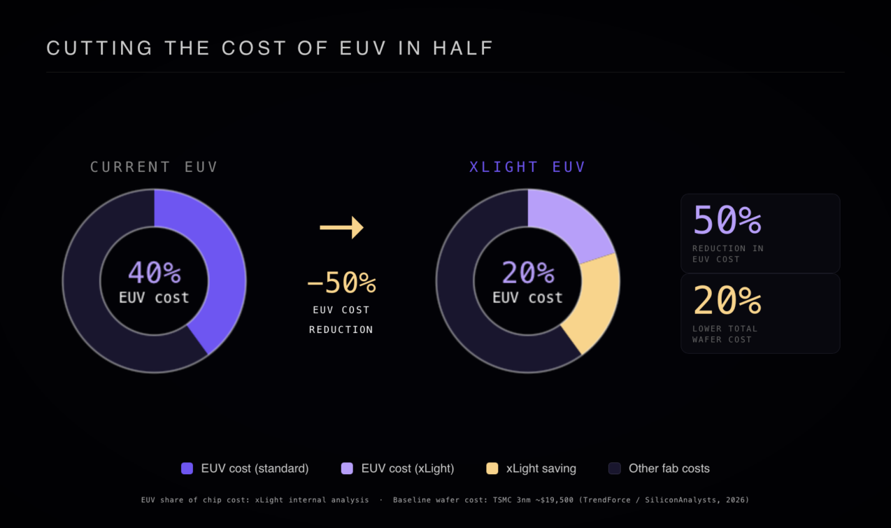
Source: xLight Inc. -
Returning the United States to dominance in semiconductor fabrication
The United States must create a new type of more vertically-integrated foundry to continue pushing Moore’s Law in both performance and cost. And we’re finally on our way.
Substrate in October 2025:
Substrate was founded to return the United States to dominance in semiconductor fabrication on three core beliefs:
- The cost of semiconductor fabrication is out of control, and it will only continue to trend upward without radical new technological innovation
- The United States is dangerously reliant on sources of geopolitical and supply chain risk that we do not directly control
- The only chance the United States has to return to dominance in semiconductor production would be to create a new type of more vertically-integrated foundry, one that continues pushing Moore’s Law in both performance and cost
To achieve this, Substrate is building next-generation semiconductor fabs to return America to dominance in semiconductor production and will use our technology—a new form of advanced X-ray lithography—to power them.
Meanwhile, SpaceX two days ago:
Earlier this year, SpaceX and Tesla announced Terafab – the most epic-chip building effort in the world – combining logic, memory and advanced packaging all under one roof. In April, Tesla broke ground on a new research fab on the North Campus of Giga Texas – the precursor to Terafab. And today, we are announcing that Terafab will be built in Grimes County, Texas. The facility will be an advanced semiconductor fab that will bridge the divide between current global chip supply and the compute demand of the future.
[…]
The initial phase of Terafab is estimated to require approximately $16.8 billion in capital investments from SpaceX and Tesla, with potential future expansion phases bringing total investment much higher. This facility will employ at least 3,000 people, many of whom will be from Grimes and nearby Brazos County — continuing the trend of our other Texas sites where between 60% and 80% of new hires are local residents.
[…]
SpaceX and Tesla also take our role as being good stewards of the environment seriously. The Terafab site is committing to the use of Gibbons Creek Reservoir water for industrial operations rather than local groundwater; planned on-site wastewater treatment facilities; water reuse and conservation efforts; compliance with all applicable environmental and pollution control laws; and management of hazardous materials, chemicals, and industrial byproducts in accordance with all applicable regulations—while striving to exceed them.

State-of-the-art EUV Tools today
EUV photolithography is extremely complex. If you need a primer on how this process works, Branch Education has a good one:
Production of EUV light involves vaporizing molten tin droplets 50,000 times a second.
ASML:
In our laser-produced plasma (LPP) source, molten tin droplets of around 25 microns in diameter are ejected from a generator at 70 meters per second. As they fall, the droplets are hit first by a low-intensity laser pulse that flattens them into a pancake shape. Then a more powerful laser pulse vaporizes the flattened droplet to create a plasma that emits EUV light. To produce enough light to manufacture microchips, this process is repeated 50,000 times every second.
This LPP source is power intensive and not powerful enough to avoid inherent reliability problems which reduce yields.
Free Electron Laser
Unlike the laser-produced plasma source used in EUV photolithography today, a free electron laser (FEL) can produce EUV light with a fraction of the power requirements and with greater light output.
Here’s how a FEL EUV light source can transform photolithography:
As Elon says, “FEL FTW” — you can expect a next generation light source inside Terafab.
American lithography
Substrate plans to use a next generation light source:
The team at Substrate has designed a new type of vertically integrated foundry that harnesses particle accelerators to produce the world’s brightest beams, enabling a new method of advanced X-ray lithography. Our accelerators create and power beams that generate light billions of times brighter than the sun, directly into our lithography tools, each using a completely new optical and high-speed mechanical system to produce the smallest of features needed for advanced semiconductor chips.
While current approaches are reaching their limits, leading to increasing costs and complexity, all of our inventions are designed to work together to extend Moore’s Law for years to come.
Our light source begins with radio-frequency cavities accelerating pulses of electrons using powerful electric fields. The electrons ride each successive wave, gaining energy and increasing their velocity to near the speed of light. To produce light, these charged, highly energetic electrons traverse a gauntlet of strong alternating magnetic fields, which force them to release their energy as bursts of brilliant, intense light. These bright pulses of light are transported and shaped by a succession of perfectly polished optics all the way to the silicon wafer.
Not just the light source, but everything:
Our team has designed, fabricated, and polished optics, formulated marvels of chemistry, machined and assembled tons of metal to produce a new type of advanced lithography built from the ground up for high-volume manufacturing—a feat of engineering no one thought possible for a startup.
Over the past several years, we have invested in building out our supply chain and continue to increase our vertical integration, enabling us to move at speeds usually unimaginable in the semiconductor industry. More recently, we completed our first in-house production-quality 300 mm wafer lithography tool, which operates at the extreme G-forces required to meet the throughput of a leading-edge fab.
An American-made solution to increase domestic wafer production while reducing production costs is needed:
The semiconductor industry stands at a crossroads. China has made advanced semiconductor production a national priority, investing unfathomable sums into domestic tooling and manufacturing advances. We may soon witness a similar tectonic shift in semiconductor production where technological capabilities and leadership ability abruptly change, leaving us as a country scrambling to respond to capabilities we never anticipated emerging so rapidly.
By the end of this decade, either America or China will control the future of computing and the AI industries built on top of it.
For years, many have spoken of the need for a new pure-play American foundry, yet view it as an impossible task. History repeatedly shows that American science and engineering solve impossible tasks. As we rush to build more current-generation semiconductor fabs in America today, we need to start immediate work on building the semiconductor fabs of tomorrow.
The stakes are too high for the United States not to try everything we can to solve both one of our most significant technological gaps and our biggest opportunities to reclaim leadership over the technologies we pioneered. If China surpasses the United States in advanced semiconductor production, it would fundamentally shift global technological and economic power, giving China dominant leverage over critical supply chains that power everything from AI to military equipment.
We stand on the shoulders of the American giants who built this industry. Shockley. Moore. Noyce. Grove. Chang. Huang. We want you to join us in making the next century and future of Moore’s Law an American one.
Substrate continues to make progress with an announcement in April of advancements which reduced costs and improved speed of semiconductor simulation and printing. This is used to reduce process steps and predict and avoid defects like bridging.
Building & Investing in the future
While Substrate is privately held, you can now invest in SPCX. My wife and I are shareholders. We want to see the United States return to dominance in semiconductor fabrication. We bet SpaceX will succeed. I hope Substrate does too. We want to see Americans — yet again — solve the impossible and make the next century and the future of computing an American one.